牛津仪器集团成员

Fast etch rates and clean overheads mean higher tool uptime. Higher uptime means more wafers through your fab
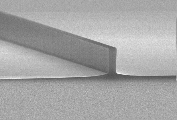
Vertical facets means higher device efficiency – more light out for power in
Smooth surfaces means less light – more usable light
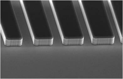
Essential with such complex structures, stopping in the right layer can make or break your device
Uniform etch depth means that more devices can be made from each wafer, improved yield decreases costs

The plasma processing toolkit for InP laser diode production
© 牛津仪器 2024
 公安机关备案号31010402003473