Author: Dr Harm Knoops
This weekend the ALD/ALE conference will start in South Korea and as always I am looking forward to the meeting. The yearly ALD conference has become a tradition for me as it is the main stage for news on ALD/ALE developments and insights on how to deposit and remove with atomic scale precision. Furthermore it is a great place to meet colleagues and friends from over the world. I am excited from my Instruments Plasma Technology (OIPT) role because of interesting new developments and applications ongoing and many nice ways in which people are using our systems. Furthermore I am excited from my part-time Eindhoven University of Technology (TU/e) role since great is expected and great discussions, not only for ALD but also for ALE and combinations thereof. In this blog I will look ahead at some of the talks and possible trends I expect. I have resisted the urge to be complete and very scientific when addressing these.
It is difficult to judge which applications are drawing the most attention. One aspect which I think is common for many -end applications is the desire for controlled deposition of -quality materials with an emphasis on control over interfaces and defects. In this respect power electronics are a nice example where both ALD and ALE have great potential in improving reliability plus enhancing device performance. In general, by bringing together the ALD and ALE community many interesting options are on the table. ALE is a prominent example, and ion energy control which is somewhat common in plasma etching is being explored in plasma ALD as well. Ideas on cleaning, smoothening and other ways of combining both ALD and ALE are present as well.
Such combinations bring me to the topic of Atomic Scale Processing (ASP), which I expect will become more prominent with the overlapping of deposition and etch communities.
Quite some contributions on ALE will be presented from people using our systems with contributions from OIPT, Lawrence Berkeley National Laboratory, TU/e, University of Glasgow and Jet Propulsion Laboratory. Interestingly these are obtained on a wide range of systems (both ALE and ALD), contain both plasma and ALE, which show both anisotropic and isotropic etching. ALE has become a broad it seems. Dr. Mike Cooke will discuss in his tutorial on the Sunday the impact of ALE on process tool and the other talks mentioned will be on the Monday and the Tuesday.
Another subject which I believe we can label as a trend is area-selective ALD. Adrie Mackus from TU/e will have an invited talk on using cycles to achieve area-selective ALD. Most striking to me in these cycles is that plasma ALD can be utilized for area-selective ALD and furthermore that it is an example where combining deposition with etching brings new possibilities. For more check out our previous blog "Area Selective ALD"
Another technique which OIPT pioneered which is gaining traction (although I might be too close to this one to call it) is applying substrate biasing during plasma ALD. I counted five contributions using our FlexAL systems ranging from ion energies to ion energies and from , nitrides, to carbides. I find it interesting to see how substrate biasing can provide properties we have not been able to attain by any other means in ALD.
Also materials which we have highlighted before will be presented. We introduced the FlexAL configuration last year. In April a paper on MoS2 deposition was published which used the FlexAL in Eindhoven, and at this conference Shashank Balasubramanyam will present the control of WS2 properties during plasma ALD. Good to see how growth by ALD and sulfide ALD in general are picking up steam.
Besides achievements in new processes and improved properties I still cherish pure scientific developments as well. My PhD student Karsten Arts will present conformality studies investigated by lateral aspect ratio structures. Interesting personal note, 8 years ago I went to the ALD conference in South Korea as a PhD student and presented on conformality studies as well, so good to see that the pursuit to understand conformality is alive and kicking.
So for those going, see you at the conference and note that if you have any question during the conference on ALD or ALE or just want to say hi please find me or one of my colleagues at our booth or anywhere around. Below a list of the contributions which as far as I know use our systems (there are probably more):
ALE:
ALD:
For more on Instruments Plasma Technology applications visit our page or drop us a line through our email Plasma-experts@oxinst.com.

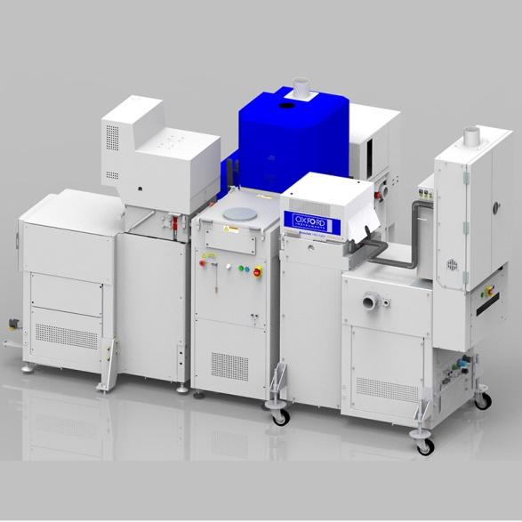
PlasmaPro Cluster for atomic scale processing CVD (for growth), ALE and ALD with load lock
Ask a question 公安机关备案号31010402003473