牛津仪器集团成员
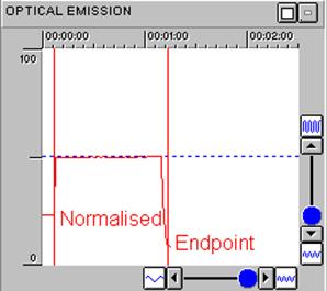
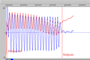
Endpoint detectors are an important tool for achieving optimal process results. Upgrade now and receive multiple benefits.
Endpoint detector upgrades currently available are:
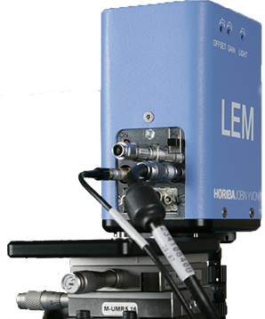
Endpoint detectors are an important tool for achieving optimal process results.
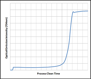
Endpoint detectors are an important tool for achieving optimal process results.
© 牛津仪器 2024
 公安机关备案号31010402003473