牛津仪器集团成员
扩展

Growth of Aligned Carbon Nanotubes (CNT)

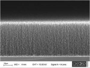
The growth of 1D materials such as carbon nanotubes offers the potential for their use in new applications such as: improving the proporties of paint; biosensors and fine filters. Instruments provides process solutions for a wide variety of 1D materials growth.

  • 600°C - 900°C
  • Plasma can be used as the pre-treatment step to facilitate or activate the catalyst particles
  • The properties of carbon nanotubes, such as the diameter and density can be controlled through the choice of the suitable catalyst and process conditions. The growth rate and uniformity of the carbon nanotubes is also related to the choice of catalyst and process conditions.
  • Load-locked system offers higher throughput, as no cooling of the growth chamber is required to exchange samples
  • The He purge gas is required for the process
  • The catalyst may be vapour generated from solid or liquid precursor through additional delivery line, not included
  • The morphology of carbon nanotubes is high density (dense bush style) depending on the catalyst
了解更多信息

Growth of inorganic nanowires as well as carbon nanotubes with in situ catalyst preparation and activation.

  • Deposition typically 400-630°C
  • Selective growth at desired positions can result from accurate positioning of catalyst particles prior to growth
  • H2 plasma can be used as the pre-treatment step to facilitate or activate the catalyst particles
  • Growth of Si nanowires is related to the catalyst and growth conditions
  • Growth is enabled using both plasma-assisted and modes
  • growth is possible using catalyst nanoparticles, without need for sputtered films
  • Load-locked system offers higher throughput, as no cooling of the growth chamber is required to exchange samples
  • The He purge gas is required for the process
  • Zinc Oxide (ZnO) is a direct band-gap (E.g.=3.37eV) with a large excitation binding energy (60meV)
  • ZnO exhibits near UV emission, transparent conductivity and piezoelectricity
  • Moreover, ZnO is biocompatible and can be used for biomedical applications without coating

Applications

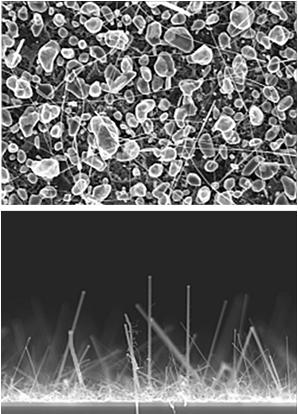
ZnO nanowires and nanorods are good candidates for nanometre scale electronic applications, such as sensors or emission transistors, because of their sensitivity to the chemical environment. The sensing process is related to oxygen vacancies on the that influence the electronic properties of ZnO.

ZnO nanowires and nanorods are also potentially good candidates for nanometre scale photonic device applications, ultraviolet photo-detectors and light emitting devices. Both p-type ZnO nanowires and n-type ZnO nanowires can be produced as positively and negatively charged semiconducting materials, this forms good foundation to make light emitting diodes (LED), in which, as an electron meets a hole, it falls into a lower energy level and releases energy in the form of a photon of light.

ZnO nanowires and nanorods can be used for fabrication of solar cells that can be dye-sensitised using liquid or solid (hole conductor) electrolyte, because ZnO has a wide bandgap, charge carrier mobility and can give a area for efficient dye-sensitization and light harvesting.

ZnO nanowires and nanorods can promote catalyst reactions with light as energy source, i.e. they can be used as photocatalysts.

The biocompatibility of ZnO nanowires and nanorods along with their electro-optical properties makes them suitable for active biomedical devices.


相关产品

沪ICP备17031777号-1 公安机关备案号31010402003473