牛津仪器集团成员
Gallium Nitride (GaN) is an exciting that is enabling key advances in some important technologies. GaN Brighntess LEDs (HBLEDs) have already revolutionised lighting, GaN laser diodes are used for speed data transmission while GaN based RF devices will soon be applied for efficient power transfer and mobile phone base stations. GaN may be dry etched using Inductively Coupled Plasma (ICP), Reactive Ion Etching (RIE) or Ion Beam Etch (IBE). It can be deposited using ALD.
Process expertise applied to demonstrate excellent roughness with damage and optimised etching rate.
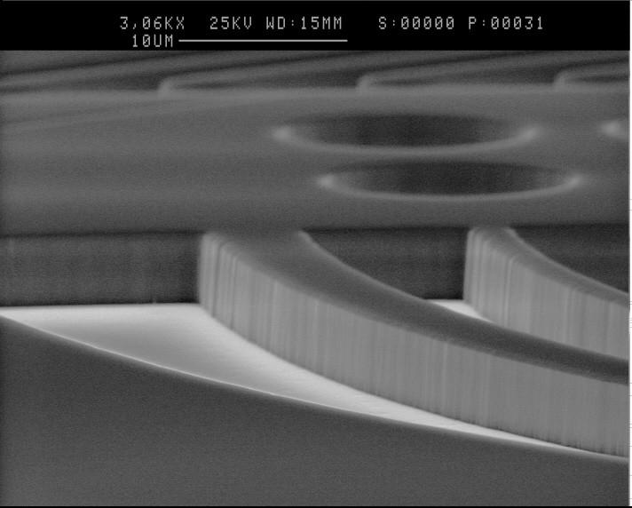
Anisotropic profile achieved at competitive etching rate.
Good control of profile with excellent selectivity.

© 牛津仪器 2026
 公安机关备案号31010402003473