牛津仪器集团成员
扩展
Collapse
牛津仪器
应用
产品
新闻
市场活动
联络我们
投资者关系
招聘岗位
新闻
市场活动
联络我们
cn
en
jp
cn
en
jp
投资者关系
招聘岗位
关于我们
设备
新闻
活动
生产解决方案
研究解决方案
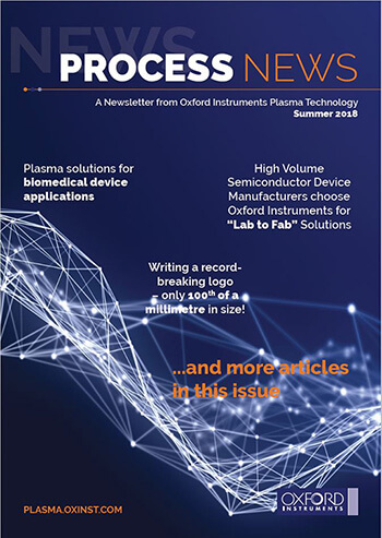
PROCESSNEWS
解决方案
二维材料
增强现实(AR)
生物器件
失效分析
HBLEDs
红外传感器
激光器
VCSELs
MEMS & 传感器
功率器件
量子技术
RF
PROCESSNEWS
工艺
等离子刻蚀
反应离子刻蚀
RIE-PE
ICP 刻蚀
等离子抛光
等离子沉积
PECVD
ICPCVD
CVD
离子束
离子束刻蚀
离子束沉积
原子层
原子层沉积
原子层刻蚀
原子层处理
材料
1D materials
2D materials
Al
2
O
3
AlGaN-GaN
AlN
a-Si
Cr
Co
Diamond
DLC
GaSb
GaAs/AlGaAs
GaN
GaP
HfN
HfO
2
InP/InGaAs/InAlAs
InSb
NbN
Ni
PMMA
Pt
Si
SiC
SiGe
SiNx
SiO
2
Ta
2
O
5
TiO
2
VO
x
ZnO
More materials...
设备
设备类型
Clusters for device production
Clusters for research
Load Lock
Open Load
Upgrades
ICP
PlasmaPro 80 ICP
PlasmaPro 100 Cobra
PlasmaPro 100 Polaris
PlasmaPro 100 Cobra GaAs VCSEL
RIE
PlasmaPro 80 RIE
PlasmaPro 100 RIE
PlasmaPro 800 RIE
Deep Si Etch
PlasmaPro 100 Estrelas
PECVD
PlasmaPro 80 PECVD
PlasmaPro 100 PECVD
PlasmaPro 800 PECVD
PlasmaPro 1000 Stratum
ICPCVD
PlasmaPro 80 ICPCVD
PlasmaPro 100 ICPCVD
ALD
FlexAL
PlasmaPro ASP
ALE
带刻蚀点的原子层刻蚀:PlasmaPro 100 ALE
离子束
Ionfab 300 IBE
Ionfab 300 IBD
纳米尺度生长
PlasmaPro 100 Nano
资料中心
博客
技术资讯
视频资料
网络课堂
云学院
白皮书
服务支持
服务与支持
服务协议
升级&软件
PTIQ 软件
备件
服务选项
培训
Teamviewer
淘汰零部件升级
联系我们
客户服务Blog & FAQS
联系我们
新闻
市场活动
联络我们
在线商城
图书馆
图书馆
增强现实技术
量子
激光
生物医学
能源&电力
故障分析
增强现实技术
用于斜面刻蚀的轮廓控制
立即阅读和下载 >
用于增强现实应用的大面积倾斜刻蚀技术
立即阅读和下载 >
量子
制造更好的金刚石和碳化硅(SiC)量子器件
立即阅读和下载 >
用于高性能量子比特的表面工程
立即阅读和下载 >
用于量子器件的原子层沉积
立即阅读和下载 >
使用太赫兹光谱技术对200毫米晶圆上等离子体原子层沉积的TiN进行非破坏性电特性表征
立即阅读和下载 >
激光
InP基激光器和光电二极管的前端等离子体解决方案
立即阅读和下载 >
VCSEL Mesa制造的先进终点控制技术
立即阅读和下载 >
高产量制造GaAs基VCSEL中的Mesa
立即阅读和下载 >
高功率VCSEL阵列的干法刻蚀
立即阅读和下载 >
InP激光二极管器件的生产:定义Mesa
立即阅读和下载 >
InP激光二极管器件的生产:等离子体沉积以实现最佳性能
立即阅读和下载 >
InP激光二极管器件的生产:DFB光栅刻蚀以实现最佳性能
立即阅读和下载 >
生物医学
生命科学和生物医学应用的器件制造:屏障和生物相容性涂层
立即阅读和下载 >
生命科学和生物医学应用的器件制造:电气、光子和微机电系统(MEMS)器件
立即阅读和下载 >
生命科学和生物医学应用的器件制造:疏水、亲水和功能性表面的制备
立即阅读和下载 >
生命科学和生物医学应用的器件制造:微流体组件制造
立即阅读和下载 >
能源&电力
为电力电子应用中实现可靠的常关型凹栅MISHEMT制造
立即阅读和下载 >
等离子体抛光:高规格的碳化硅(SiC)表面处理
立即阅读和下载 >
氮化镓功率电子器件的原子层沉积和原子层刻蚀
立即阅读和下载 >
用于制造碳化硅功率器件的全球领先等离子体加工解决方案
立即阅读和下载 >
Cells原子层沉积(ALD):朝着稳定高效的钙钛矿太阳能电池迈进
立即阅读和下载 >
等离子体工艺:实现高性能氮化镓/碳化硅(GaN on SiC)射频器件的关键步骤
立即阅读和下载 >
故障分析
高效且精确:等离子体工艺技术在故障分析中的应用
立即阅读和下载 >
在新选项卡中打开
沪ICP备17031777号-1
公安机关备案号31010402003473
 牛津仪器集团成员

 公安机关备案号31010402003473