牛津仪器集团成员
Silicon Oxide (SiO2) in its variety of forms is an essential for , MEMs and optoelectronic devices. Quartz is used in gratings for Augmented Reality (AR); Doped are used for waveguides and SiO2 can be used for device passivation. SiO2 may be deposited and etched using several technologies:
The PlasmaPro 100 Polaris brings together unique Electrostatic Clamp (ESC) technology along with our well established Cobra300 ICP source. This delivers excellent repeatability while maintaining etch rate and profile quality.
Process optimised for excellent control of profile at optimised etching rate.
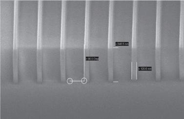
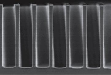
aspect ratio quality nanoscale SiO2 etch
Anisotropic and isotropic profile available at competitive etching rate with optimised uniformity.
More on RIE 了解更多信息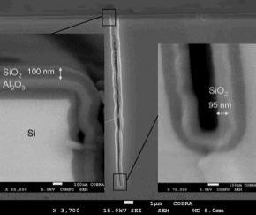
Very conformality with short cycle time (90 ms prec. and 4.5 s plasma). Courtesy TU/e
Excellent uniformity of both thickness and refractive index, and stress control available at deposition rate. Different chemistries can be used: pure and diluted silane.
SiO2 deposited using TEOS and O2 by ICP CVD in ~50μm deep trench 4:1 aspect ratio
Excellent uniformity of both thickness and refractive index. Stress control available at deposition rate. Different chemistries can be used: pure and diluted silane.
More on PECVD 了解更多信息
Excellent stoichiometry with competitive deposition rate.

© 牛津仪器 2026
 公安机关备案号31010402003473