牛津仪器集团成员
扩展

2D Materials

materials such as , MoS2 or hBN can be used to enhance current devices and build new device architectures. FETs, batteries and filters with unique proporties can now be realised.  Instruments Plasma Technology offers precise process control for mono/multi layer growth with defects.

Proven damage results.

  • >800°C
  • Load-locked system offers higher throughput, as no cooling of the growth chamber is required to exchange samples
  • He purge gas is required for the process
  • Characterization of materials is performed using techniques such as Raman and Photoluminescence to study structural and (opto) electronic quality.


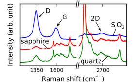
This specification is issued for obtained through Chemical Vapour Deposition (CVD) processes.

  • Load-locked system offers higher throughput, as no cooling of the growth chamber is required to exchange samples
  • He purge gas is required for the process
  • The presence of layer(s) will be tested by Raman peak analysis
  • 1 layer will be confirmed by Raman
了解更多信息
  • 600°C - 900°C
  • Load-locked system offers higher throughput, as no cooling of the growth chamber is required to exchange samples
  • He purge gas is required for the process
  • Nucleation depends on the underlying substrate and C-source combination (Carbon, 2013, Vol. 58, 59–65)
了解更多信息

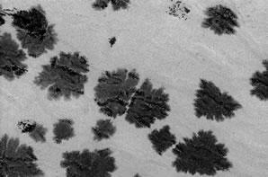
Direct growth of nanocrystalline on dielectric substrates using plasma enhanced chemical vapour deposition.

  • >900°C
了解更多信息

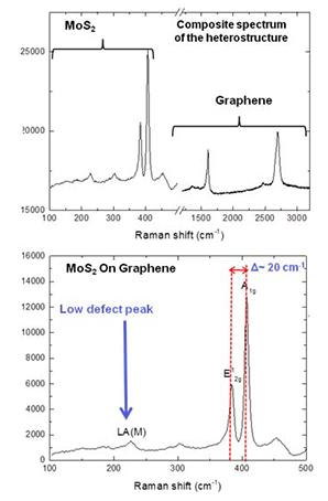
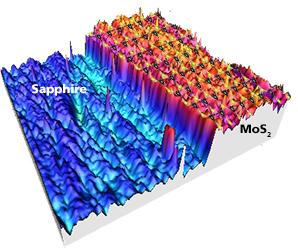
In situ growth of  Molybdenum Disulphide (MoS2) heterostructures

We offer CVD/PECVD/Remote plasma (ICP) CVD systems equipped with precursor vapour delivery modules for the growth of two dimensional layers and heterostructures of materials like , MoS2, WS2 etc. 

This is a three step process:

  • Step 1: Grow on Cu
  • Step 2: Transfer from Cu on to SiO2
  • Step 3: Grow MoS2 on transferred on SiO2

Process features:

  • >900°C
  • Formation of a single layer of MoS2 confirmed by Raman
  • Deposition time is critical to ensure that a complete monolayer of MoS2 is formed
  • of MoS2 deposition on and its quality is critical for stability of the during MoS2 process
了解更多信息

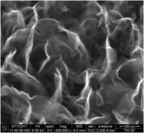
This specification is issued for Boron Nitride obtained through Chemical Vapour Deposition (CVD) processes. For the purpose of process demonstration, B2H6 is used as Boron source and NH3 as the Nitrogen sources on Cu/Ni foils as catalyst substrates.

  • >900°C
了解更多信息

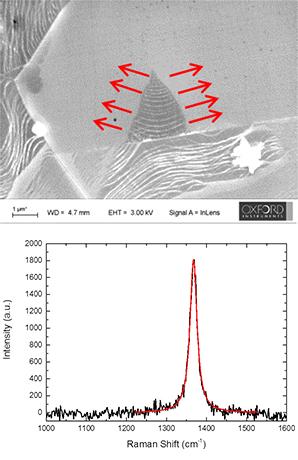
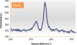
Growth of MoS2 and related Metal Dichalcogenides

We offer PECVD systems equipped with precursor vapour delivery modules for the growth of two dimensional layers of materials like MoS2, WS2 etc.

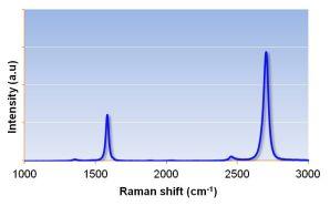
Excellent thickness control with defects and strong  photoluminescence  

quality MoS2:

  • shows defined step height and smooth uniform
  • Raman indicates one mono-layer is deposited with characteristic peaks spaced 21.1cm-1 apart
了解更多信息

相关产品

沪ICP备17031777号-1 公安机关备案号31010402003473