牛津仪器集团成员
ALE是一种先进的刻蚀技术,可以针对较浅的微结构进行出色的深度控制。 随着器件微结构尺寸越来越小,要达到器件的更高性能可以通过ALE技术所具有的精度来实现。
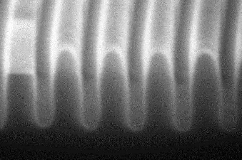
在如今的先进微电子器件制造中,高保真度的图案转移(刻蚀)是至关重要的。随着特征尺寸缩小至亚10纳米级别,以及新型器件采用超薄的二维材料,对原子尺度保真度的需求不断增加。
原子层刻蚀(ALE)技术克服了传统(连续)刻蚀技术在原子尺度上的局限性,因而受到越来越多的关注。基于等离子体的原子层刻蚀是一种气体投放和离子轰击的循环刻蚀过程,可逐层去除材料,并有潜力以极低损伤去除单层原子。
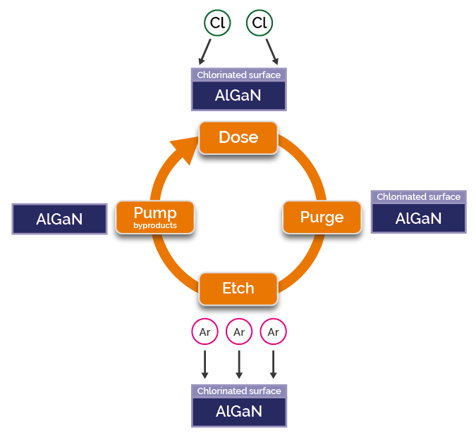
原子层刻蚀通常包括4个步骤的周期,根据需要可重复多次,以达到所需的刻蚀深度。以下是使用 Cl2/Ar进行AlGaN刻蚀的ALE示例:
步骤 1) 对基底进行刻蚀气体的投放,刻蚀气体吸附在刻蚀材料上并与之发生反应。通常,刻蚀气体经等离子体解离以增强吸附速率。通过正确选择投放气体和参数,这个步骤可以实现自限制,即在吸附一层分子后化学投放停止。
步骤 2) 清除所有剩余的投放气体
步骤 3) 用低能惰性离子轰击表面,去除已发生反应的表面层。如果离子的能量足以去除化学修饰层,但不足以(溅射)刻蚀下层块状材料,这可能是自限制。
步骤 4)清除腔室内的刻蚀产物。
原子层刻蚀有望提高基于氮化镓的HEMT的质量,并消除与高刻蚀率相关的损伤。
由Mike Cooke博士和Andy Goodyear博士为《复合半导体》杂志撰写。
ALE适用于多种材料,包括 Si、a-Si、MoS2、SiO2、GaN、AlGaN、III-V’s、Si3N4、石墨烯、HfO2、ZrO2、Al2O3和金属等。
刻蚀的材料 |
投放气体 |
刻蚀气体 | ||
MoS2 |
Cl2 |
Ar | ||
|
Cl2 |
| ||
SiO2 |
|
| ||
AlGaN or GaN |
Cl2, BCl3 |
Ar | ||
AlGaN or GaN |
N2O |
BCl3 | ||
GaAs or AlGaAs |
Cl2, BCl3 |
Ar | ||
InP or InGaAsP etc. |
CH4 |
Cl2 | ||
SiN |
H2 |
Ar | ||
Al2O3 |
BCl3 |
Ar | ||
Graphene |
O2 |
Ar | ||
HfO2, ZrO2 |
Cl2, BCl3 |
Ar |
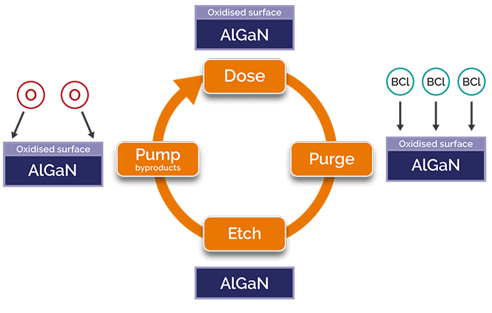
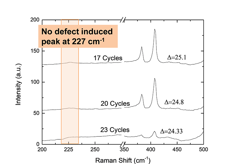
氮化镓ALE工艺周期
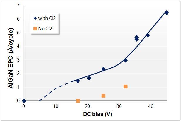
使用和不使用氯剂量时的氮化铝刻蚀周期
我们的原子层刻蚀设备拥有13年以上的丰富经验。主要特点包括:

© 牛津仪器 2026
 公安机关备案号31010402003473