牛津仪器集团成员
Plasma etching is an essential tool in today’s world, enabling many of the technologies we take for granted. For example, the smartphone would not be possible without it.
Plasma etching is a way of creating features in virtually any , the features can be on the nm scale or 100s of microns; the technique can be used to make them all.
One of the leading technologies for plasma etching is ICP-RIE it offers many advantages in process performance:
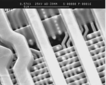
To take profile control and illustrate it’s benefits: Moore’s Law has driven device critical dimensions (CD) down to well below µm level. If you have a feature that etches in the same direction vertically and horizontally such a closely packed array of devices will soon interfere with one another.
ICP-RIE plasma etching can produce perfectly vertical features so CD is maintained. It is widely used compared to wet etching precisely for this reason.
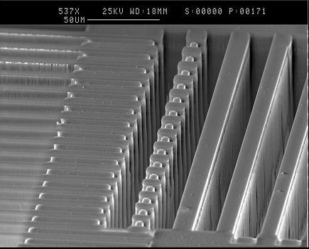
Deep Silicon Etching using ICP RIE
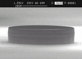
Gallium Arsenide VCSEL etching process
Plasma etching by RIE has been widely used for decades, whilst it’s performance does not match that of ICP-RIE it is a simple technique that is very effective for many applications.
Plasma etching of dielectric masks for example usually does not require rates and RIE provides sufficient verticality to create great masks.
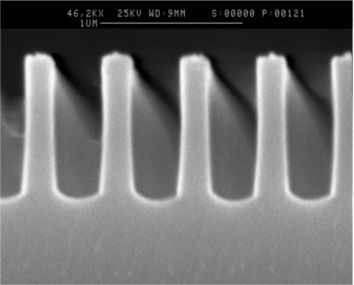
Silicon Dioxide (SiO2) RIE Etching
PE etching is the least directional of the plasma etching solutions it is therefore unsuitable for creating fine, vertical features. It is used for highly selective isotropic processes where undercut is acceptable it can be useful for clearing large areas of selectively to an underlying layer.
Plasma etching is a sophisticated, versatile technology that is used to create a wide range of devices.
Failure Analysis using PE Etching
Contact us at plasma-experts@oxinst.com to find out about our process solutions for plasma etching.

© 牛津仪器 2026
 公安机关备案号31010402003473