牛津仪器集团成员
扩展

Diamond Processing

Diamond offers a set of characteristics that make it an interesting choice for a wide range of applications. It has the highest known conductivity making it attractive for heat removal, is chemically un-reactive and is the hardest known . It also has a wide (5.5eV) indirect bandgap meaning it has a breakdown voltage. It can be etched using Inductively Coupled Plasma (ICP), Reactive Ion Etching (RIE) or Ion Beam Etch (IBE).
  • As a substrate for power devices it is robust, lightweight and able to transfer heat from the active region better than any other whilst tolerating applied voltages.
  • It is a suitable replacement for silicon in MEMS devices where wear and bio-compatibility are a concern and can be combined with piezo- materials like AlN to form SAW devices. Its optical absorption is across the visible spectrum, which combined with a refractive index allows it to be used for applications like waveguiding.
  • The leading candidate for processing, where NV centres can be interrogated to give about the states.

Good control of morphology.

More on ICP 了解更多信息
  • Wafer size: up to 200mm
More on IBE 了解更多信息

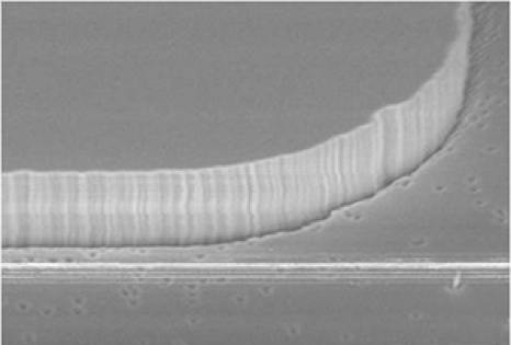
Process achieves anistropic profile and smooth surfaces .

More on RIE 了解更多信息

相关产品

沪ICP备17031777号-1 公安机关备案号31010402003473